Advanced PCB Fabrication with Strict Quality Control
| Layer & Structure | |
|---|---|
| Number of Layers | 1 - 108 Layers |
| Board Thickness | 0.2mm - 10.0mm |
| Copper Weight | 0.5oz - 10oz |
| Max. Panel Size | 600mm x 600mm |
| Min. Panel Size | 5mm x 5mm |
| Trace & Space | |
|---|---|
| Min. Trace Width/Space | 0.05mm / 0.05mm (2/2mil) |
| Impedance Control | ±10% |
| Min. Silkscreen | 0.15mm (6mil) |
| Min. Solder Mask Dam | 0.1mm (4mil) |
| Finish Copper | 35μm - 210μm |
| Drilling | |
|---|---|
| Min. Mechanical Drill | 0.10mm (4mil) |
| Min. Laser Drill | 0.075mm (3mil) |
| Max. Aspect Ratio | 20:1 |
| Via Plating Thickness | 25μm minimum |
| Buried & Blind Vias | Supported |
| Surface Finish | |
|---|---|
| HASL (Lead Free) | ✓ Available |
| ENIG (Electroless Nickel Gold) | ✓ Available |
| OSP | ✓ Available |
| Immersion Silver | ✓ Available |
| Immersion Tin | ✓ Available |
| ENEPIG | ✓ Available |
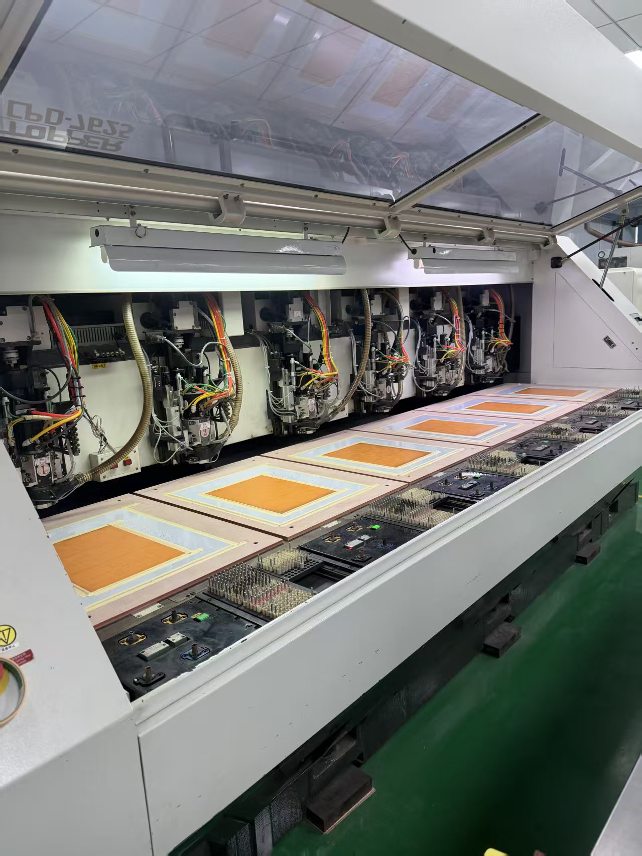
State-of-the-art CNC drilling and routing equipment for high-precision PCB manufacturing
All raw materials are inspected and tested before production. We only use certified materials from approved suppliers.
In-process quality checks at every critical manufacturing stage. Statistical process control (SPC) for consistent quality.
100% electrical testing, AOI inspection, and optional X-ray for BGA/QFN packages. IPC-A-600 Class 2/3 compliance.
Our technical team is ready to help with your PCB requirements.
Contact Us